5. Memory Hierarchy > 5-1. Cache overview
Cache overview
Updated at 2022.11.10
Memory hierarchy
Locality
- Temporal locality
- Items accessed recently are likely to be accessed again soon
- Spatial locality
- Items near those accessed recently are likely to be accessed soon
Memory structure
- SRAM (cache memory attached to CPU)
- Fastest (o.5ns ~ 2.5ns)
- most expensive
- smallest
- DRAM (main memory)
- Faster (50ns ~ 70ns)
- more expensive
- smaller
- Disk (HDD, SSD)
- Slowest (5ms ~ 20ms)
- cheapest
- largest
Use hierarchy
- Copy recently accessed (and nearby) items from disk to smaller DRAM memory
- Copy more recently accessed (and nearby) items from DRAM to smaller SRAM memory
Term
- Block
- The minimum unit of information
- It can be either present or not present in a cache
- Hit
- Accessed data is present
- Hit ratio: # of hits / # of accesses
- Miss
- Accessed data is absent
- Block is copied from lower level (Additional time taken)
- Miss ratio: # of misses / # of access (= 1 - hit ratio)
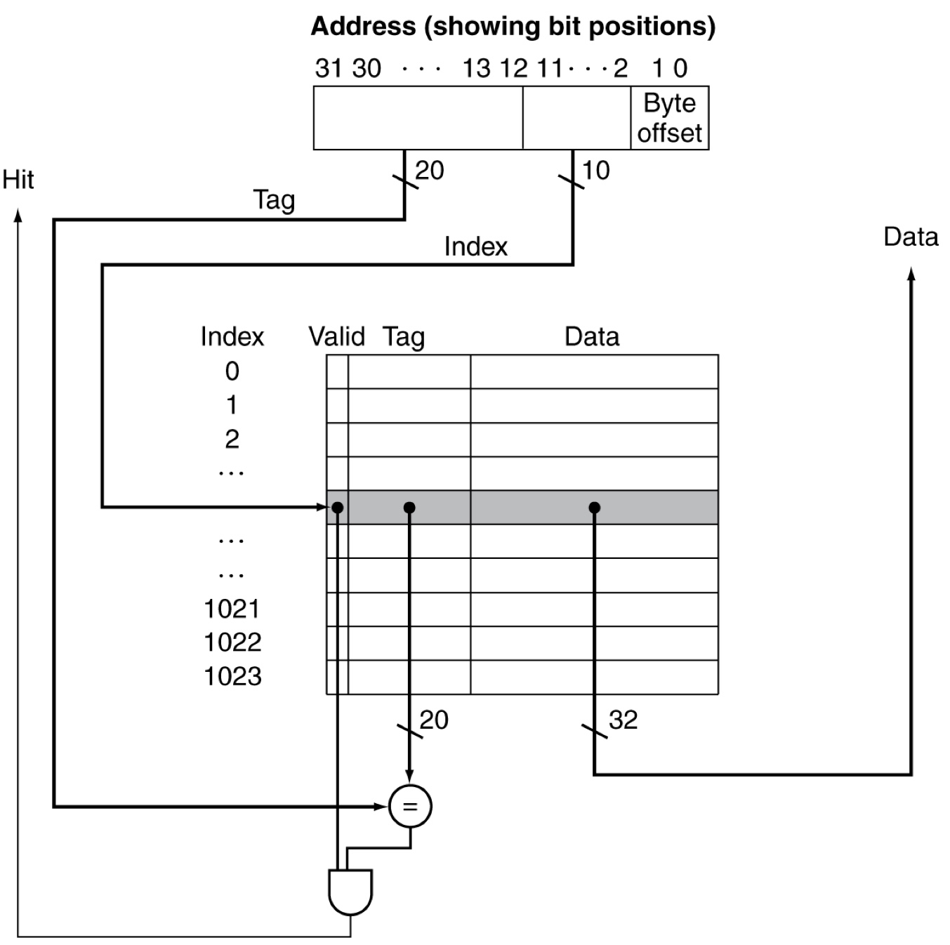
Direct mapped cache
Each memory location can be mapped directly to exactly one location in the cache
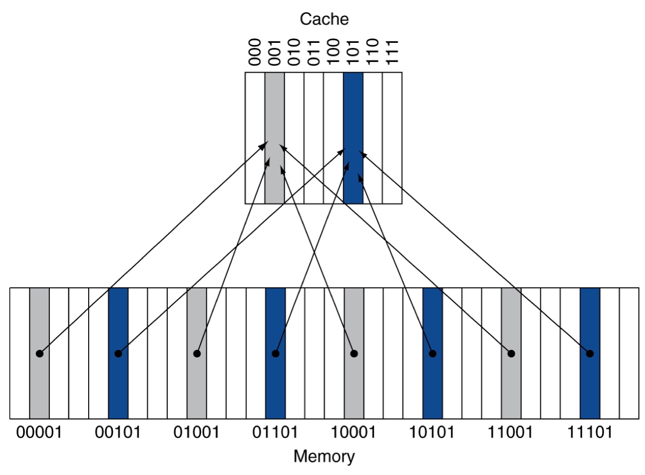
- Cache address = (Block address) modulo (# of blocks in cache)
- Num of blocks in cache is power of 2 (e.g., 2, 4, 8, 16, 32, ...)
- The cache address is determined by the low-order bits of block address
- Tags contain the address information of the data (the high-order bits of the address)
- To avoid using meaningless information, add a valid bit for each cache block
- Valid bit = 1 (the cache block contains valid information)
- Valid bit = 0 (the cache block contains invalid information)
- Initially, the valid bits of all cache blocks are set to 0
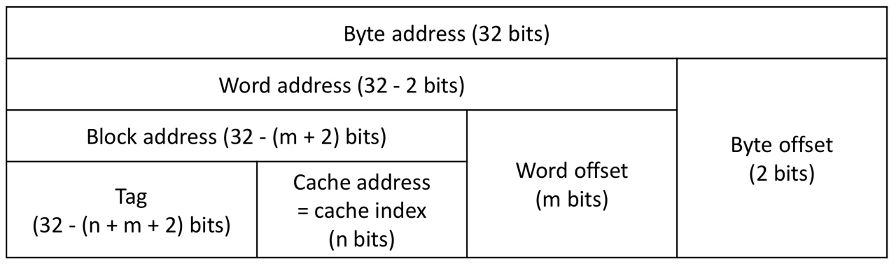
Cache address
- 32-bit addresses
- num of cache blocks: blocks (the lowest n bits of the block address are used for the index)
- Block size: words ( bytes)
- m bits are used for the word within the block, 2 bits are used for the byte within the word
Cache size
Cache size
= Cache table size
= Num of cache block (valid bit length + tag length + block size(data length))
Practice 1
- 32-bit addresses
- Num of cache blocks: blocks
- Block size: words ( bytes)
Cache size
=
= bits
Practice 2
- 32-bit addresses
- Num of cache blocks: 64 blocks
- Block size: 4 words
Cache size
=
= bits
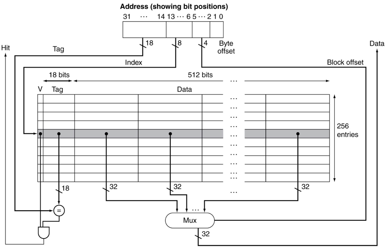
More about
- If we increase the size of blocks, this may help reduce miss rate due to spatial locality
- But, Larger blocks -> a smaller number of cache blocks -> more competition -> increased miss rate
- Increased miss penalty (the time for copying from lower level)
Handling cache misses
On cache hit, CPU proceeds normally. (requiring 1 clock cycle
But, on cache miss, the control unit of the CPU
- Step 1: stalls the CPU pipeline
- Step 2: copies a block from the next level of hierarchy (e.g., memory)
- Step 3: does the stalled task
- Restarts instruction fetch (IF stage)
if the cache miss happened when fetching an instruction from the instruction memory - Completes data access (MEM stage)
if the cache miss happened when loading data from the data memory
- Restarts instruction fetch (IF stage)
Handling writes
When will the newly-updated data in the cache be written to the lower-level memory (e.g., main memory)
- Write-through: Update both cache and lower-level memory at the same time
- Write-back: Just update cache
- Keep track of which block is dirty (used)
- When a dirty block is replaced, write it back to the lower-level memory
| Pros | Cons | |
|---|---|---|
| Write-through | - Consistency between cache and memory is guaranteed - Easy to implement | - Slow write speed |
| Write-back | - Fast write speed (if there is no replacement) | - Consistency between cache and memory is not guaranteed - Complex to implement |
Write-through with write buffer
To reduce the delay of write operations on the write-through method,
we can use a write-buffer (much faster to access than memory)
- A write buffer folds data waiting to be written to lower-level memory
- Step 1: Update both cache and write buffer
- Step 2: The processor continues the program execution without waiting
- The memory takes the updated data from the write buffer
- If the buffer is full, the processor must stall until there is an empty position
The write buffer can be also used to improve the performance of write-back
- If all the blocks in cache are dirty
Handling write misses
If there is no requested block in the cache, it causes write misses
- Write-allocate
- First, fetch the block to cache
- And then, handle the write operation
- Write around
- Just update the portion of the block in lower-level memory, but not put it in cache
- It is good when we need to initialize memory space
Real-world example
Embedded MIPS processor with 12-stage pipeline
- Split cache: I-cache (for instructions) and D-cache (for data)
- Each 16KB: 256 blocks 16 words per block
Cache performance
CPU time = clock cycle clock period
= (CPU execution clock cycles + memory-stall clock cycles) clock period
- CPU execution clock cycles
- The clock cycles that CPU spends executing the program
- Cache hit time is included
- Memory-stall clock cycles
- The clock cycles that CPU spends waiting for the memory access
- Mainly from cache misses
Memory-stall clock cycles
Simplifying assumption: the read and write miss penalties are the same
Num of memory accesses Miss rate Miss penalty
= Num of misses Miss penalty
In MIPS, we have two different cache (instruction (I-cache) and data (D-cache))
Num of memory accesses Miss rate Miss penalty
= Num of instruction memory access I-cache miss rate I-cache miss penalty
Num of data memory access D-cache miss rate D-cache miss penalty
Practice 1
- Base CPI (on cache hit) = 2
- Instruction-cache miss rate = 2%
- Data-cache miss rate = 4%
- Miss penalty = 100 cycles
- Load & stores are 36% of instructions
Miss-stall clock cycles (when there are I instructions)
- For instructions: I 0.02 100 = 2 I
- For data: I 0.36 0.04 100 = 1.44 I
CPU time
- Actual CPU time: (2 I + 2 I + 1.44 I) clock period = 5.44 I clock period
- Ideal CPU time: (no cache misses = perfect cache): 2 I clock period
Practice 2
Suppose the processor is made faster, but the memory system is not
- Base CPI (on cache hit) = 2 -> 1
- Instruction-cache miss rate = 2%
- Data-cache miss rate = 4%
- Miss penalty = 100 cycles
- Load & stores are 36% of instructions
| Memory-stall clock cycle | Memory-stall CPI | |
|---|---|---|
| For I-cache | 2 I | 2 |
| For D-cache | 1.44 I | 1.44 |
| CPU time | CPI | |
| Actual | 4.44 I CP | 4.44 |
| Ideal | 1 I CP | 1 |