5. Memory Hierarchy > 5-2. Improving cache performance
Improving cache performance
Updated at 2022.11.17
Associative caches
Support more flexible placement of blocks
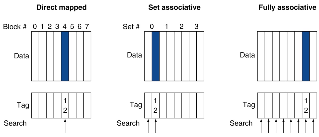
Fully associative cache
- A cache structure in which a block can be placed in any location in the cache
- Requires all entries to be searched
N-way set associative cache
- A cache that has N locations where each block can be placed
- Requires N entries to be searched
- The set containing a memory block
(Block address) modulo (num of sets in the cache) - Direct-mapped cache = 1-way set associative cache
- Full-associative cache = M-way set associative cache
(where M is num of cache blocks in the cache)
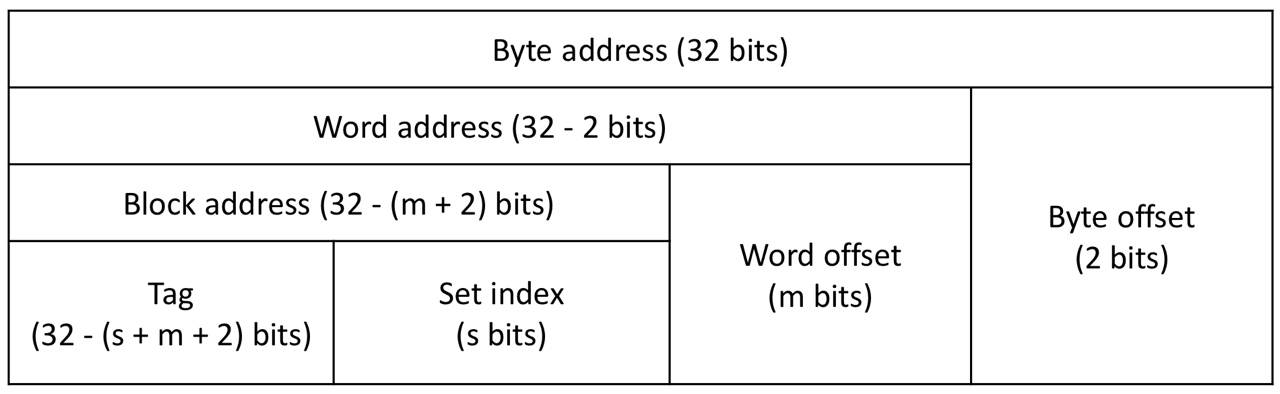
Associative cache address
- 32-addresses
- num of cache blocks: blocks
- num of sets in the cache: sets (each set contains blocks: -way set associative cache)
- Block size: words ( bytes)
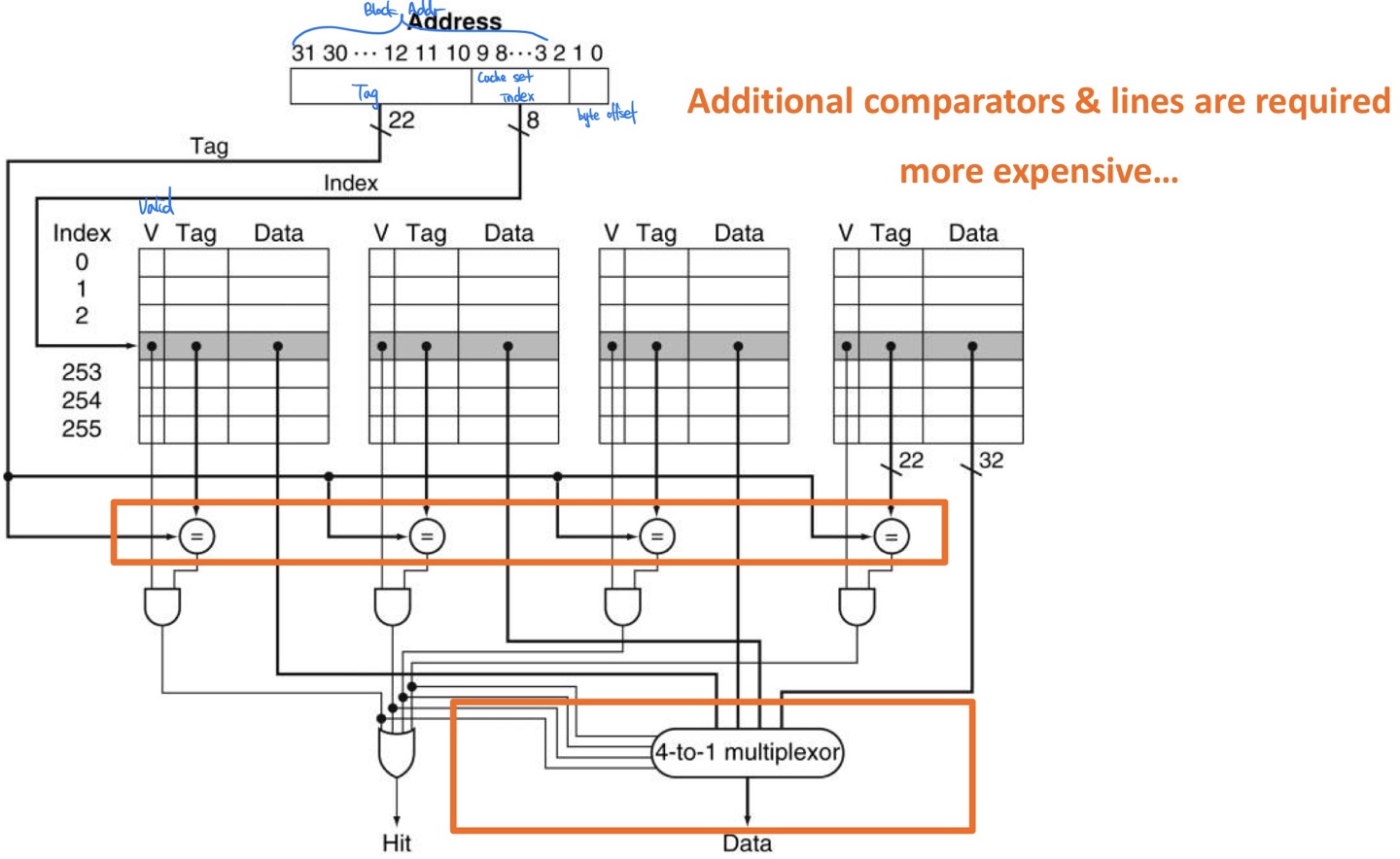
Implementation of 4-way set associative cache
How much associativity
Increasing associativity makes flexibility & complexity increase.
We have to find moderate amount of set size.
Block replacement policy
In set associative cache, if we have to make room for another block, one of blocks in a cache set must be removed
- Find non-valid entries and replace one of them
- If there are no non-valid entries, then choose one of valid entries in the set based on
- Least-recently used (LRU)
- Random
Multi-level caches
Use primary (level-1, L-1) and secondary (level-2, L-2) caches
- L-1 cache: placed close to (attached to) CPU
- Small, but very fast
- L-2 cache: placed a little bit far from CPU
- Accessed on L-1 cache misses
- Larger and slower than L-1 cache, but still faster than main memory
- Main memory is accessed on L-2 cache misses
Practice 1
- CPU base CPI = 1
- L-1 miss rate = 2%
- Main memory access time = 100ns
- Clock period = 0.25ns
CPI of a single-level cache system = CPU base CPI + memory stall CPI
= CPU base CPI + L-1 miss rate * main memory access clock cycles
= CPU base CPI + L-1 miss rate * main memory access time / clock period
=
=
Practice 2
- CPU base CPI = 1
- L-1 miss rate = 2%
- Global miss rate = 0.5% (Both L-1 & L-2 are missed)
- L-2 access time = 5ns
- Main memory access time = 100ns
- Clock period = 0.25ns
CPI of a 2-level cache system = CPU base CPI + memory stall CPI
= CPU base CPI + L-1 miss rate * L-1 miss penalty + global miss rate * L-2 miss penalty
= CPU base CPI + L-1 miss rate * L-2 access time / clock period + global miss rate * main memory access time / clock period
=
=
Considerations
Designing L-1 cache
- Focus on minimizing hit time -> to yield a short clock period
(the MEM stage time & IF stage time are determined based on the L-1 cache hit time)
Designing L-2 cache
- Focus on minimizing miss rate -> to avoid main memory
Therefore, in multilevel caches,
- L-1 cache and its blocks size is smaller than a single-level cache
- to reduce hit time and miss penalty
- L-2 cache is larger than a single-level cache
- to reduce miss rate